Wednesday, July 23, 2025 at 2pm
Defense of doctoral thesis by Gaëlle BIGEARD, for the University Grenoble Alpes, speciality " NANO ELECTRONIC & NANO TECHNOLOGIES "
Keywords:
Quantum charge transport, Nanoelectronics, Density functional theory, Green's functions
Abstract :
The goal of this PhD is inscribed in the problematic of understanding the resistive switching of two-terminal, vertical metal|2D material|metal devices. Such devices have been found to have at least two non-volatile resistive states, which are yet to be fully parametrized. In order to understand the resistive switching of these systems, one must first define all the possible high-resistance states and low resistance states. The first step to do that, is to simulate pristine systems only, and then add defects. The aim of this thesis is to establish a database of such pristine metal|2D material|metal devices, which will serve as a stepping stone for future works.
Following this goal, the electronic properties of metal|2D material|metal stacks are calculated using density functional theory, and their conductance is calculated via the non-equilibrium Green function formalism. The simulations are conducted using three local Linux servers, along with the GRICAD, TGCC, and IDRIS Jean Zay servers for over 4 million CPU.hours. The work is divided into three main databases: a material, a device, and a transport database.
The material database is used to get the electronic properties of the individual materials (band structure, density-of-states and lattice parameter), and find the correct simulations parameters (basis, real and reciprocal grids). We study electrodes made of gold, silver, copper, nickel, platinum, chromium, and titanium nitride. The chosen 2D materials are hexagonal boron nitride, graphene, and transition metal dichalcogenides using molybdenum, tungsten, sulfur, selenium and tellurium. Both the semiconducting 2H and metallic 1T phases are simulated.
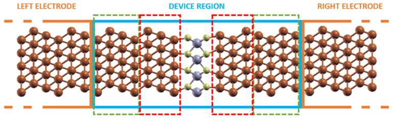
The device database is used to get the electronic properties of the metal|2D material|metal devices. This database uses directly the properties and simulation parameters of the previous database. It provides the Schottky barrier (using fat bands, vacuum level, and density-of-states), existence of mid-gap states (up to metallization), and junction tunneling barriers. Each device is made of two materials: the electrodes of the same species with crystallographic orientation (111), and one to four layers of a single 2D material. The results show that the 2D material electronic properties are strongly modified when in contact with an electrode: mid-gap states appear, the density-of-states is shifted in energy and deformed. The stronger the bonding energy at the contacts, the greater these modifications are, and the smaller are the tunneling barriers.
The transport database calculates the current going through each relaxed device of the device database. This database requires some additional optimizations. The conclusions are in accordance with the results of the device database: changing the relative in-plane position of the electrodes to the 2D material, the electrode material, or the 2D material, changes by less than an order of magnitude the conductance. Only changing the number of layers of the 2D material changes significantly the conductance. About an order of magnitude in the conductance is lost per added layer. This behavior depends on the original electronic properties of the 2D material (isolating, semiconducting, or metallic). Therefore, the simulated channel resistance is higher than the contact resistance, and the contact resistance is small (about one tenth of the conductance of the electrodes). While the contact resistance is mostly controlled by the 2D material - electrode junction distance, the channel resistance is however fully controlled by the choice of the 2D material.
These results do not follow the experimental literature, where not only the contact resistance is much higher, but also much higher than the channel resistance. The most plausible explanation is in the junction distance: increasing that distance by one angstrom is enough to divide the conductance by ten.
Jury members :
- M. Francis BALESTRA, CNRS : Supervisor
- M. Yannick DAPPE, CNRS : Rapporteur
- M. Stephan ROCHE, Institut catalan de recherche et d'études avancées : Rapporteur
- M. Mairbek CHSHIEV, Université Grenoble Alpes : Examiner
- M. Henri HAPPY, Université de Lille: Examiner
Date infos
Wednesday, July 23,2025 at 2PM
Location infos
Room M001 PHELMA / MINATEC
3 rue Parvis Louis Néel 38016 GRENOBLE Cedex 1