Responsable / Headed by
Context and Aims
The continual size reduction of active devices, together with emerging new materials (SOI, nanowires, nanotubes, etc.), leads to new properties such as quantum effects, etc. In addition, nanostructuration enhances the volume/suface ration and the sensitivity of charge carrier transport at the interfaces, such properties could be exploited for sensor applications, while it could affect the devices properties in the case of microelectronic application.
Our objectives is to study the electrical and mechanical properties of nanostructures and micro/nanosystems (MEMS/NEMS), in order to forecast possible applications in integrated circuits.
Indeed, such sensors/actuators or new nano-devices could be implemented on a chip, providing thus additional functionalities (More Moore / Beyond Moore'). It is also a way to interconnect micro/nanoelectronics with other fields such as mechanics, biology, chemistry, energy, etc.
Nano-objects are realized through local, national and international collaborations.
We have developed a technique to induce very large stress on nanoobjects.
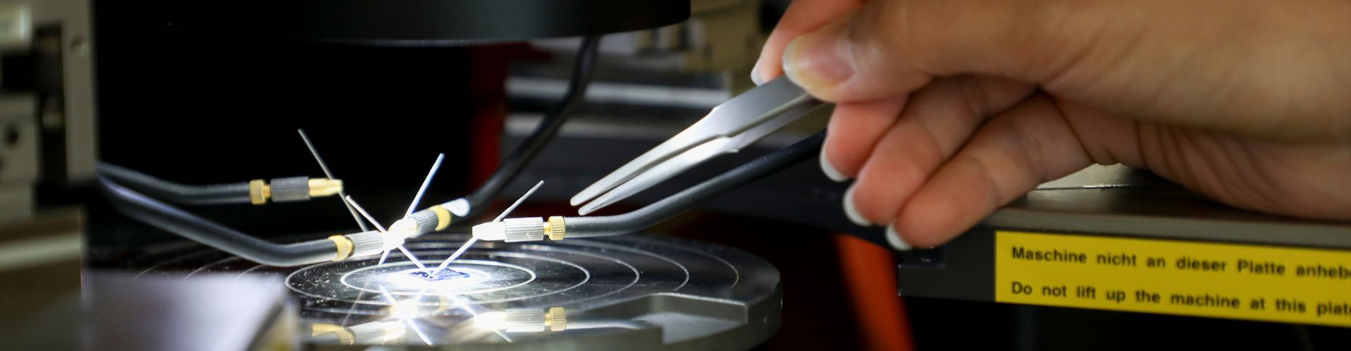
Our expertise ranges from design and simulation to prototype realisation (in clean room), and to electrical and physical characterisation.
In particular, we have developed specific simulation tools, electrical measurement systems. Upon the different equipments available in the lab, we mostly use an atomic force microscope (AFM) equipped with a XYZ feeback loop and many different electrical modes (TUNA, EFM, C-AFM, etc.), and a 3D optical interferometer for studying nanostructures in static and dynamic modes.