Context and objectives
The "Optoelectronic Techniques and Devices" axis was born from the observation that researchers from the different teams of the laboratory worked and interacted, with complementary skills, on subjects that have in common the use of both electronics and optics, electrons and photons.
These topics include those related to the design, simulation or characterization of devices (photodiodes, photocommuters, laser diodes), their use for targeted applications (such as opto-microwave and Radio on Fibre) and those interested in developing experimental techniques based on the use of optoelectronic components (such as high frequency characterization of RF circuits, or the study of quantum electronics circuits). Those research subjects are directly related to the work carried out in CMNE, RFM and PHOTO teams in the laboratory, but through this transversal axis we wanted to better highlight these interactions between teams, structure exchanges and the sharing of skills and knowledge.
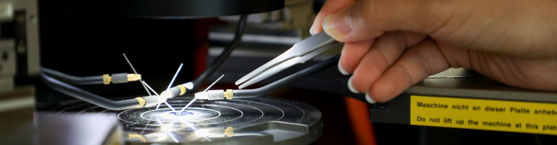
Fig. 1 : Characterization of photodetectors integrated in technology « Photonic onSilicium »
Here are some examples of research linked to this axis:
- Simulation of Ge photodiodes in Silicon Photonics technology.
- Experimental study of the ageing of optoelectronic devices.
- Influence of laser phase noise in Radio-Over-Fibre applications.
- Fast InGaAs switches for modulation and demodulation of RF signals: applications to Radio-Over-Fibre (FiWin5G Project).
- Design and characterization of high-performance GaAs fast photocommutators for quantum electronics (ANR STEPforQuBits Project).
- High-frequency characterization of RF and electronic circuits excited by optoelectronics (ANR QTERA and STEPforQuBits projects).